Cabling simulation on M3
26/may/2003: summarized by T.Takeshita
(updated 18/june/03)
________________________________________________________
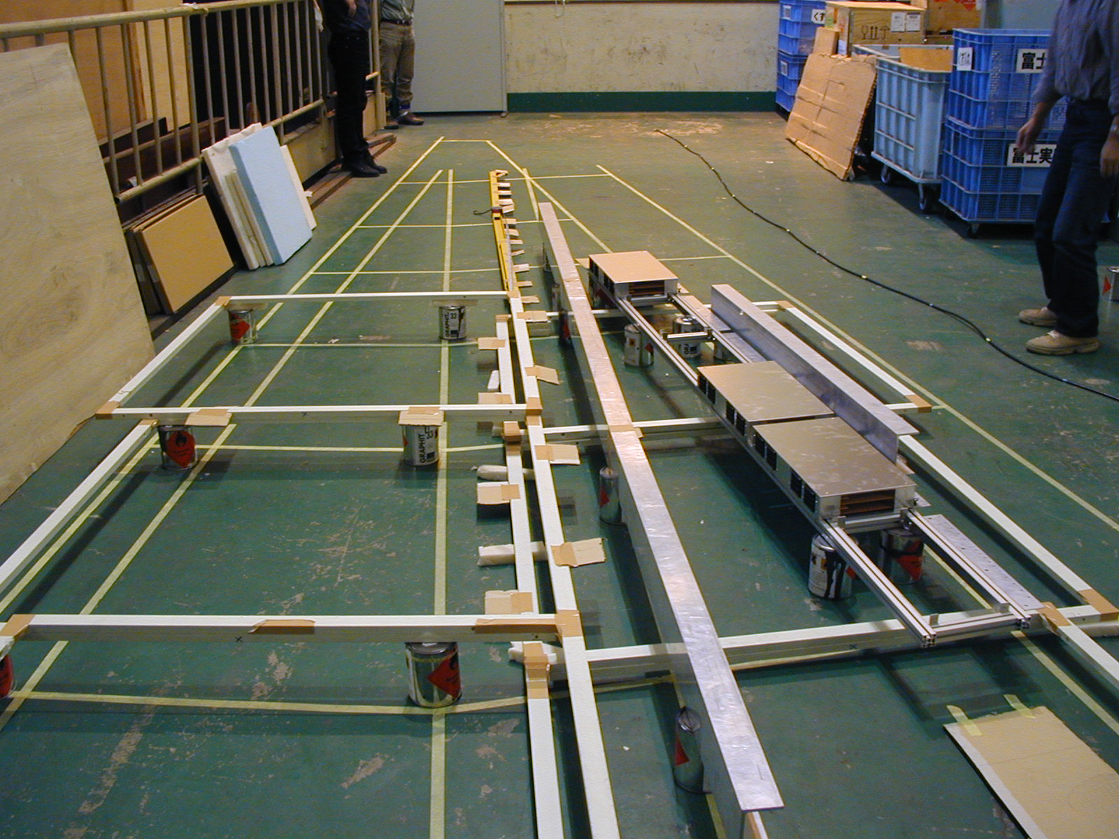
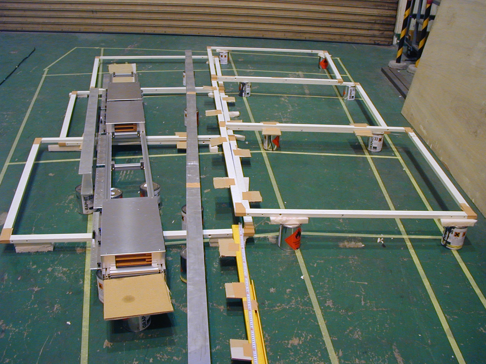
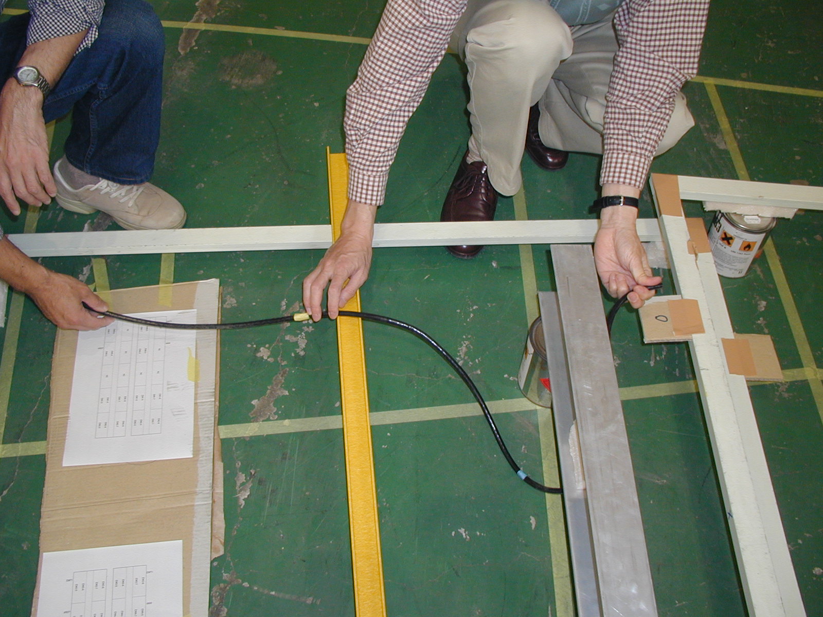
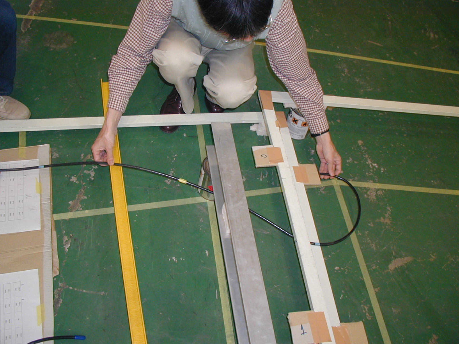
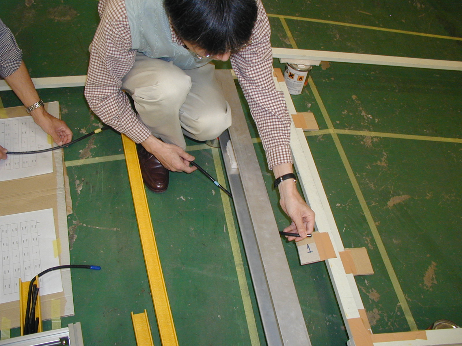
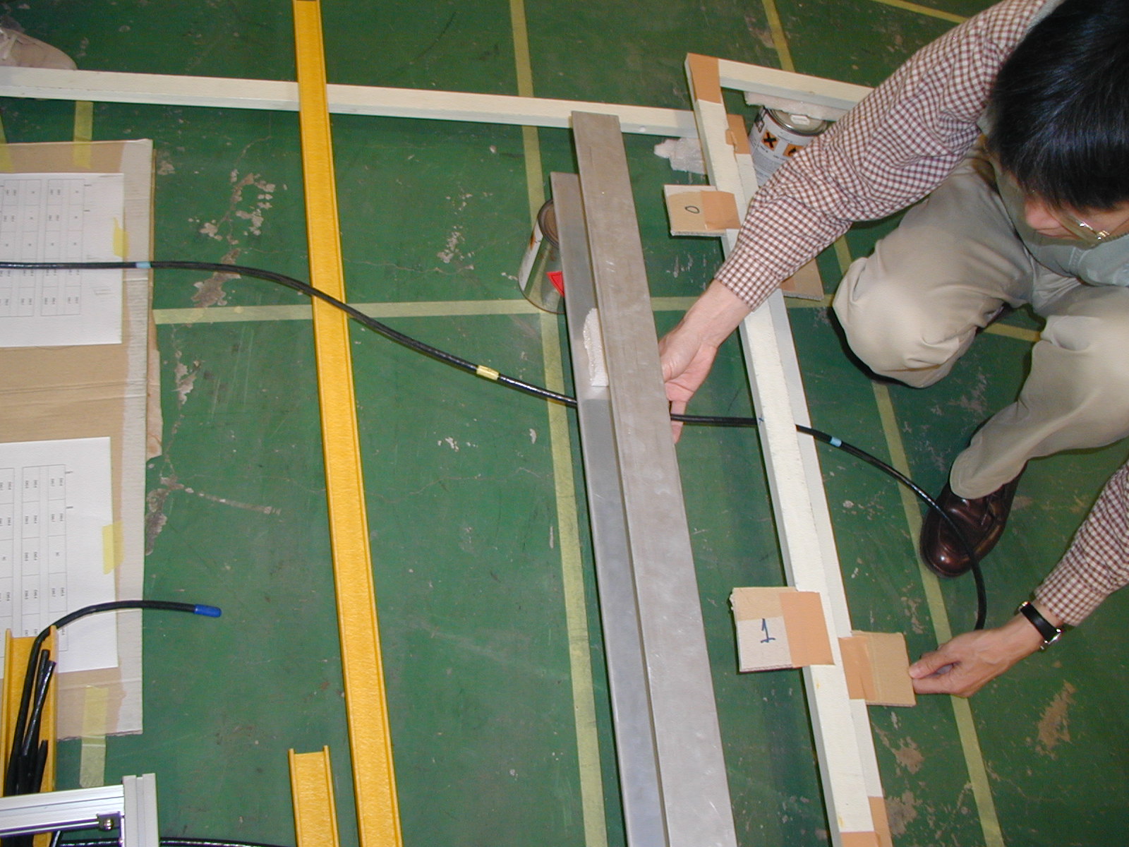
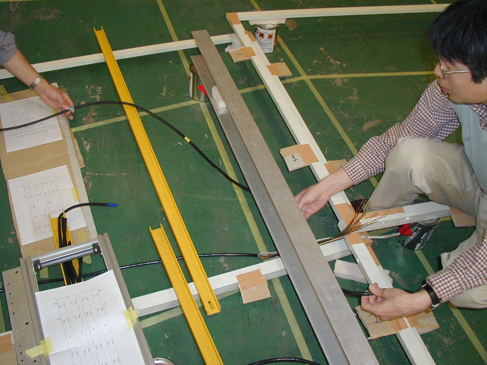
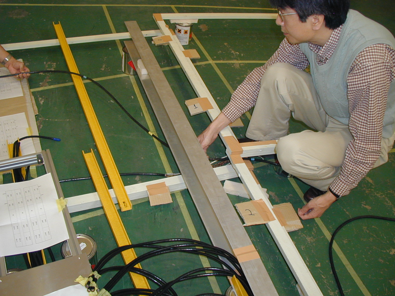
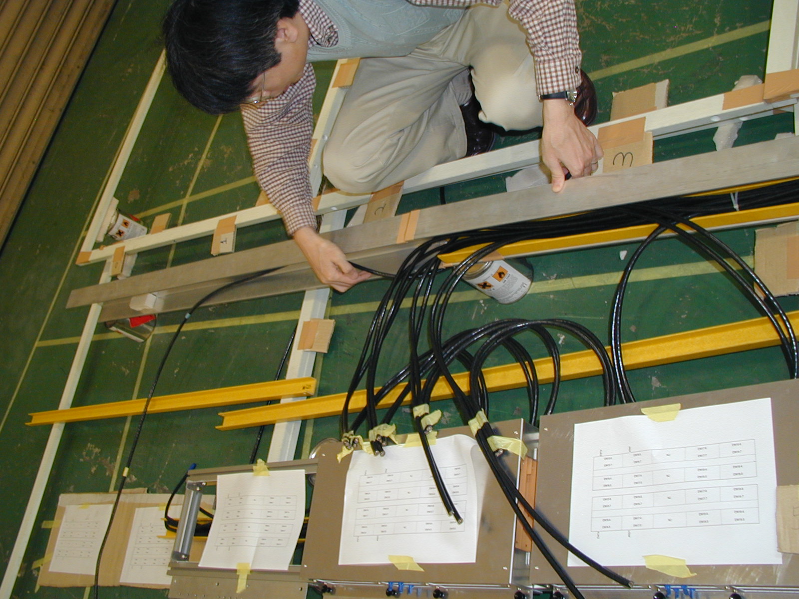
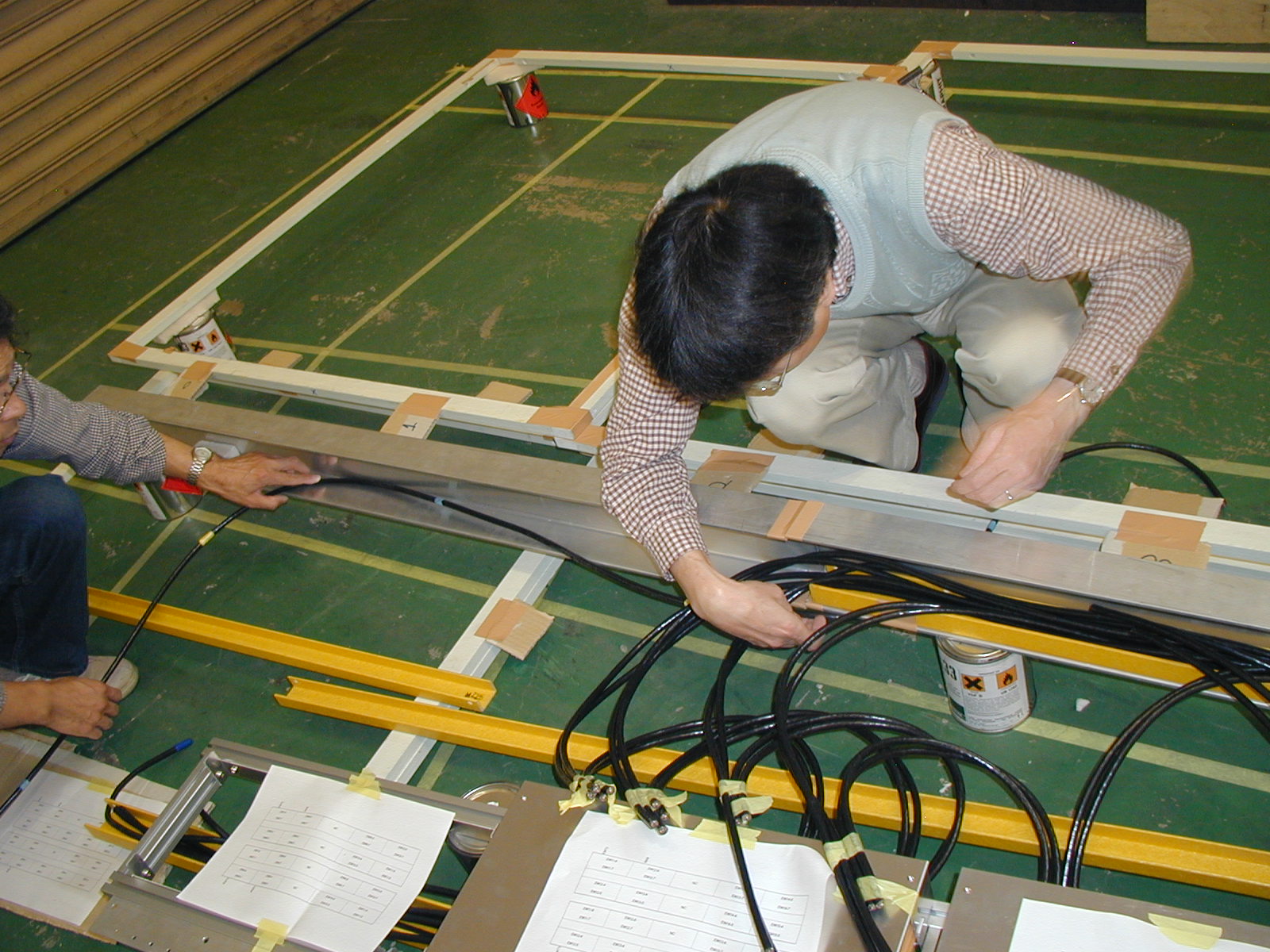
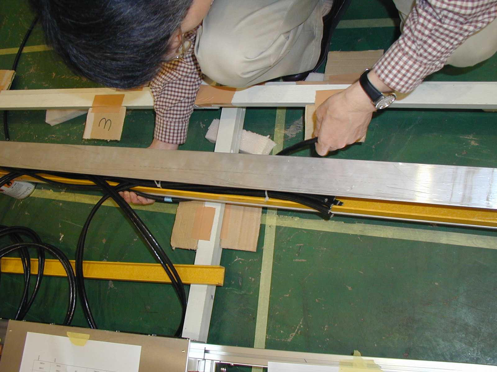
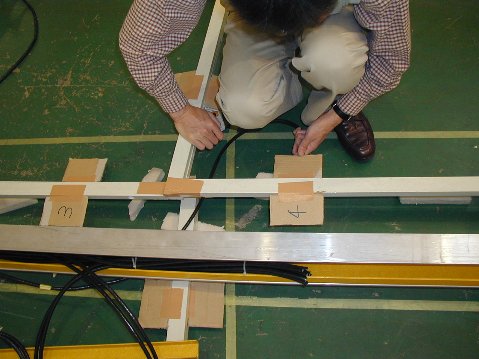
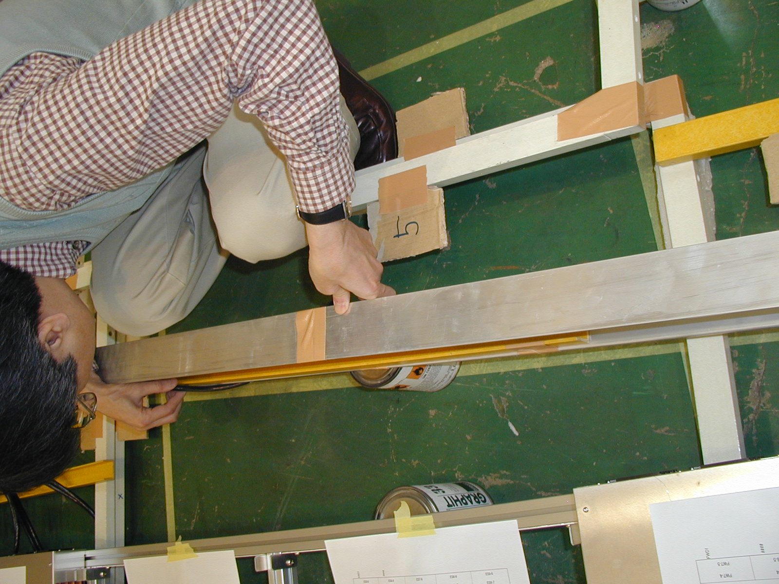
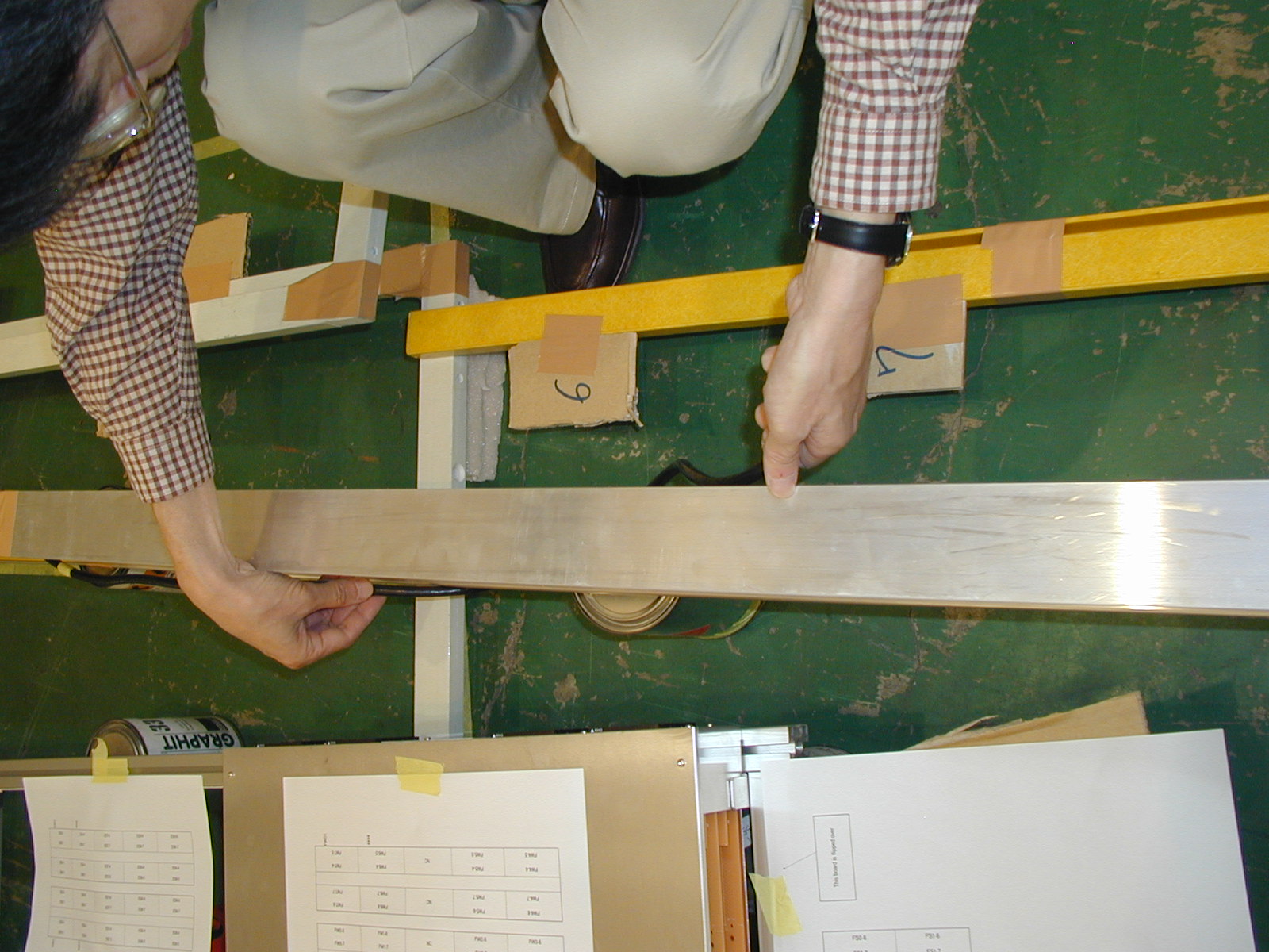
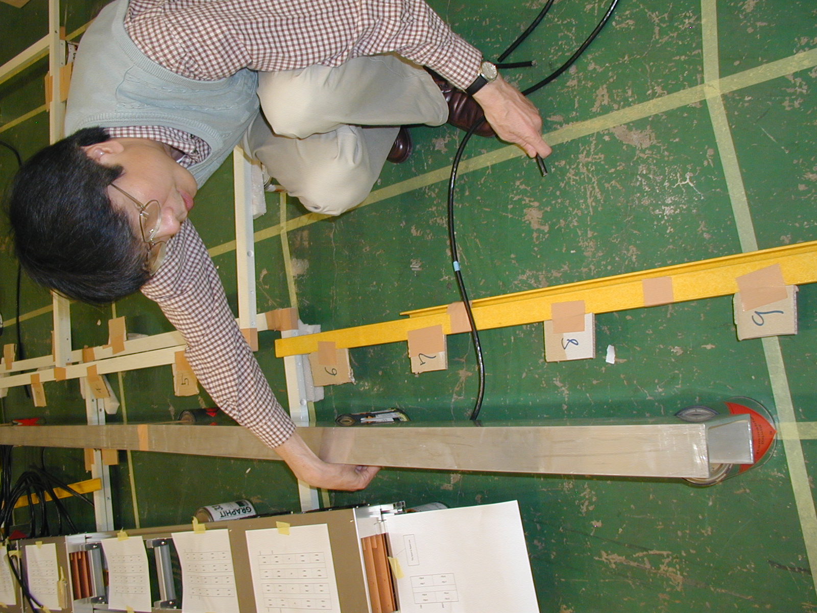
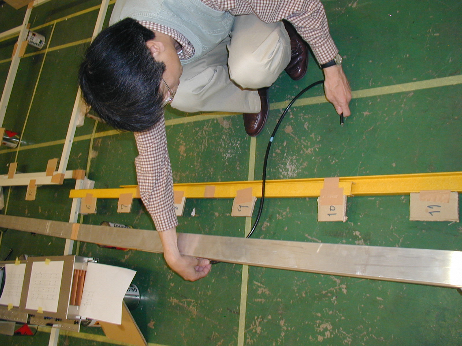
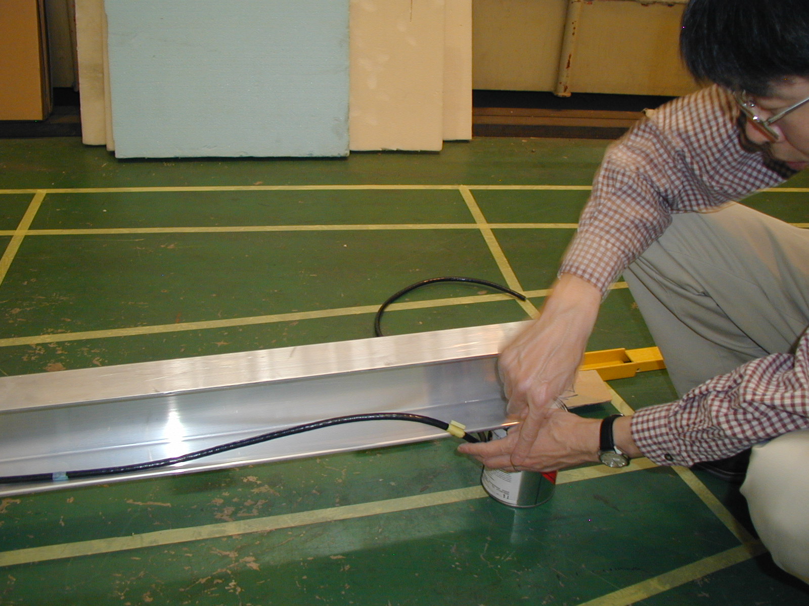
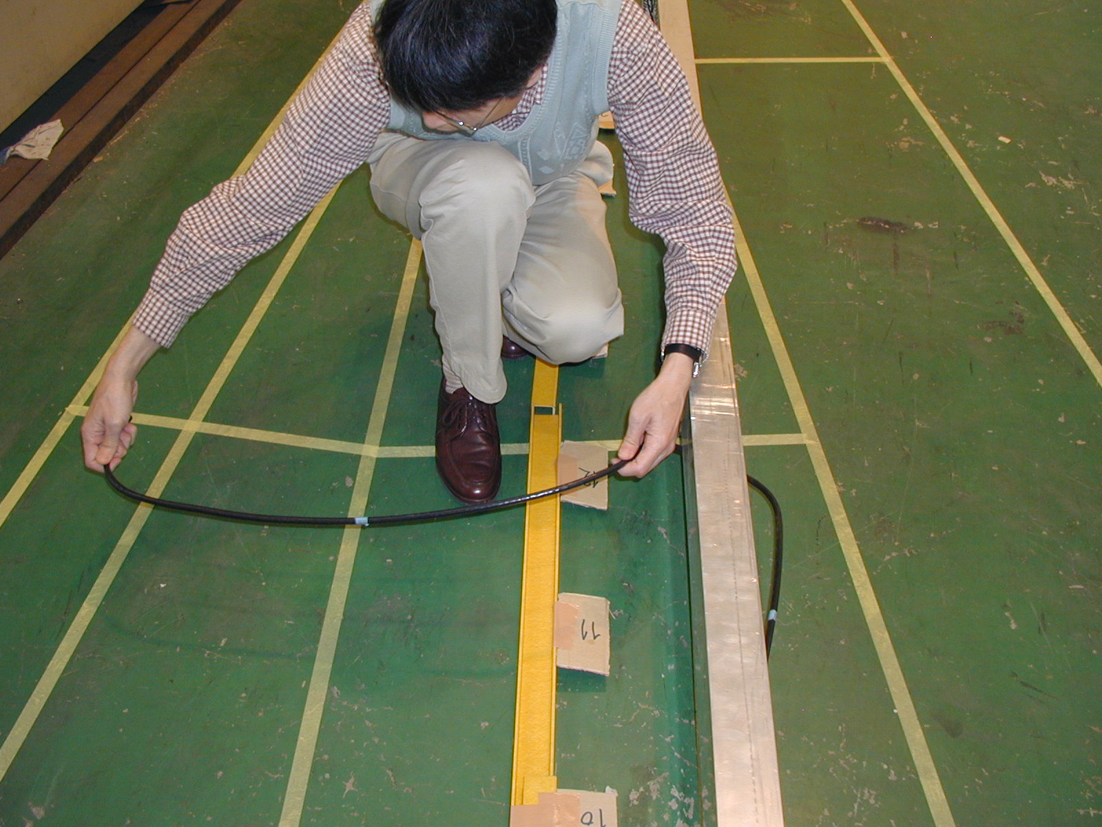
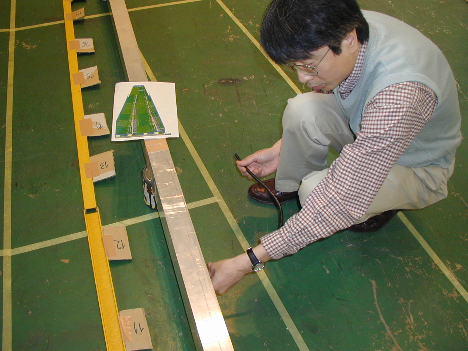
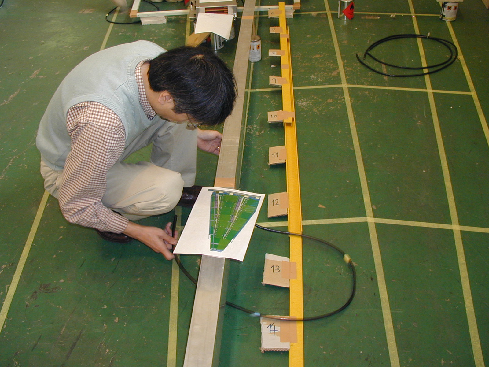
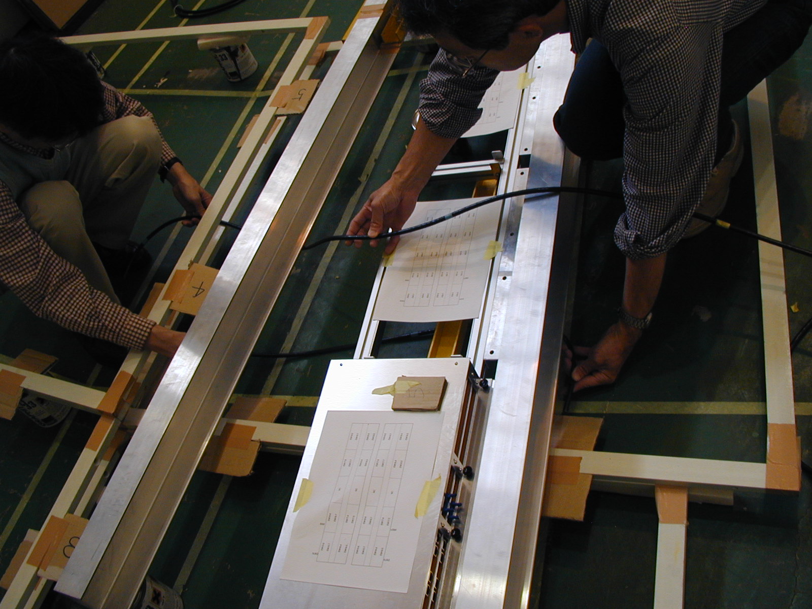
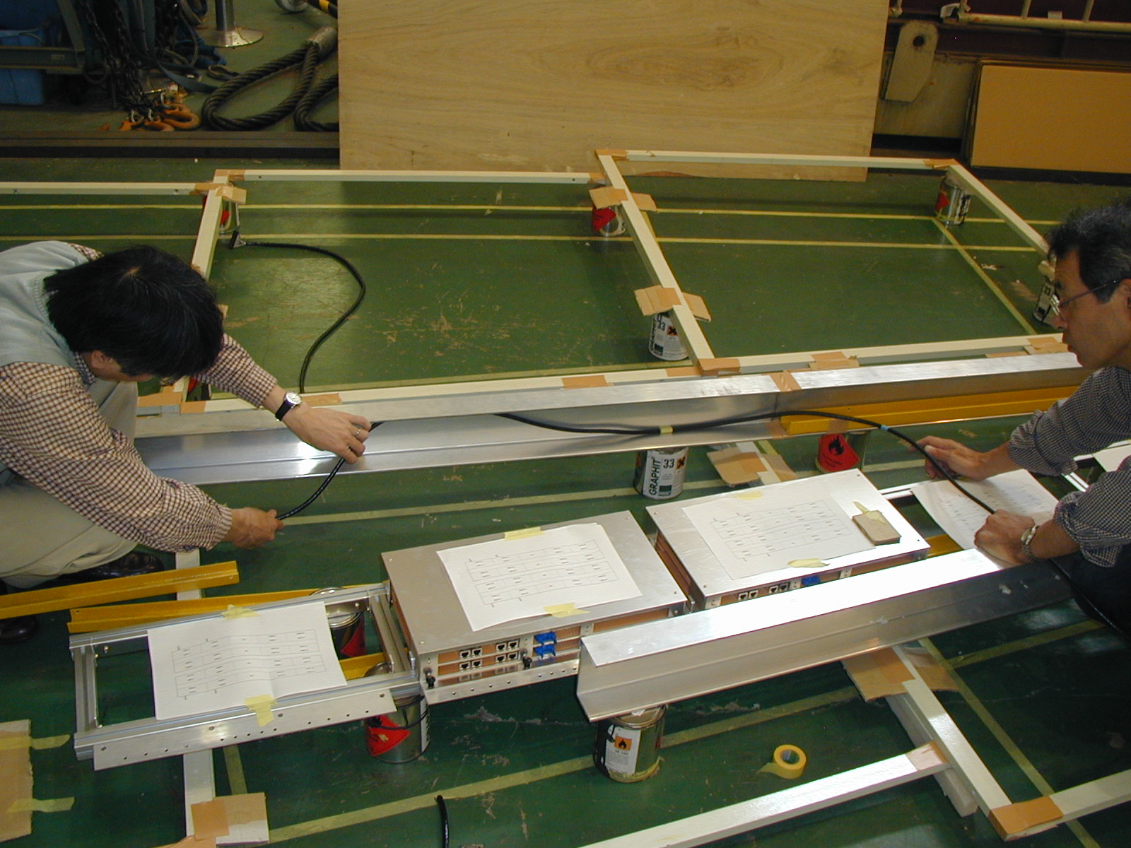
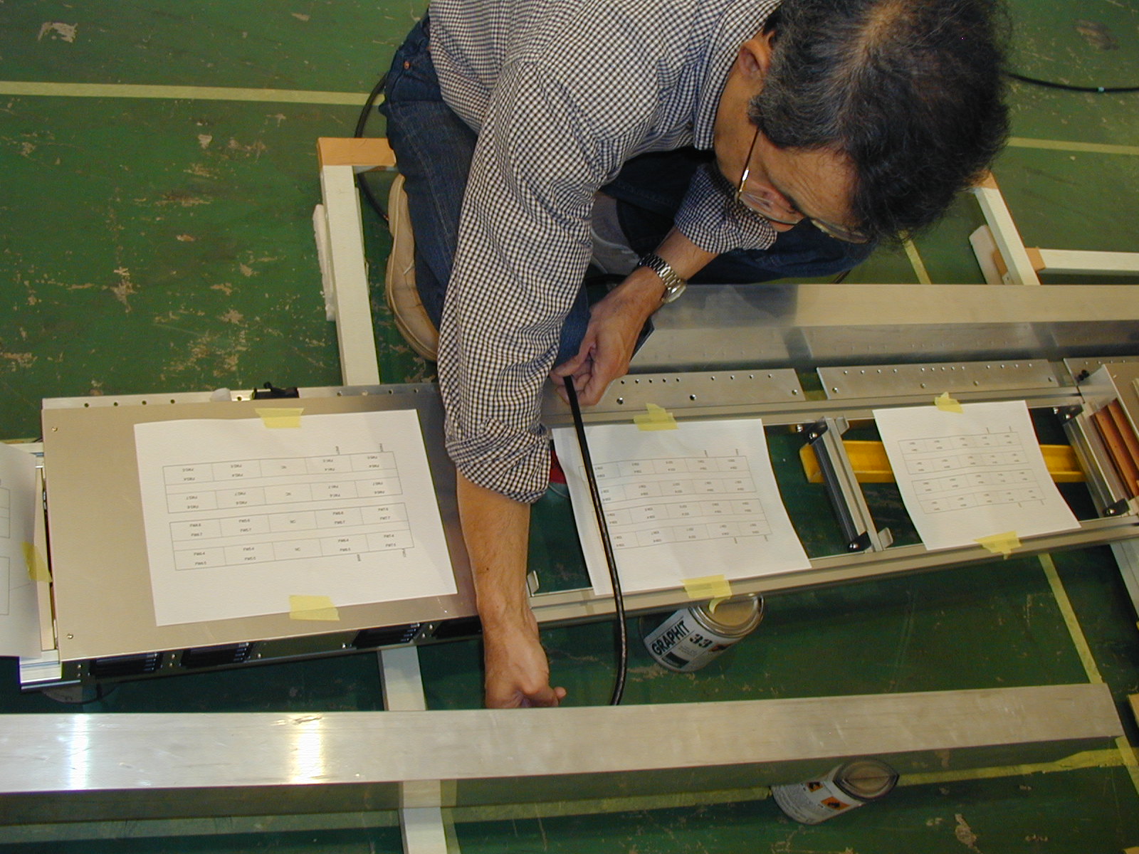
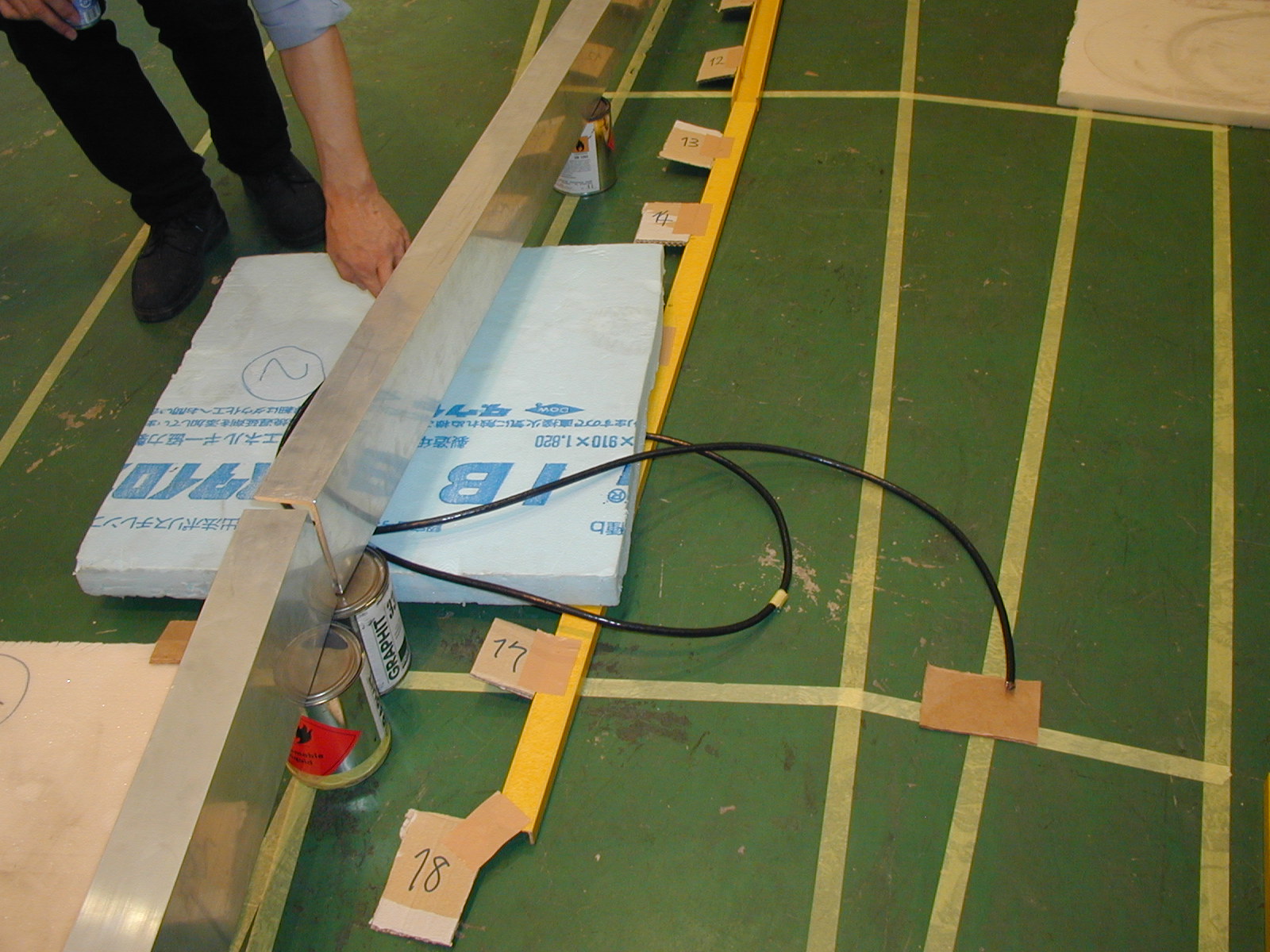
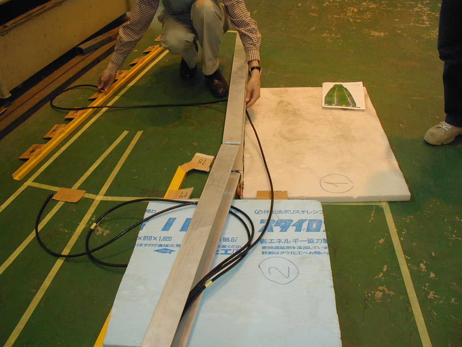
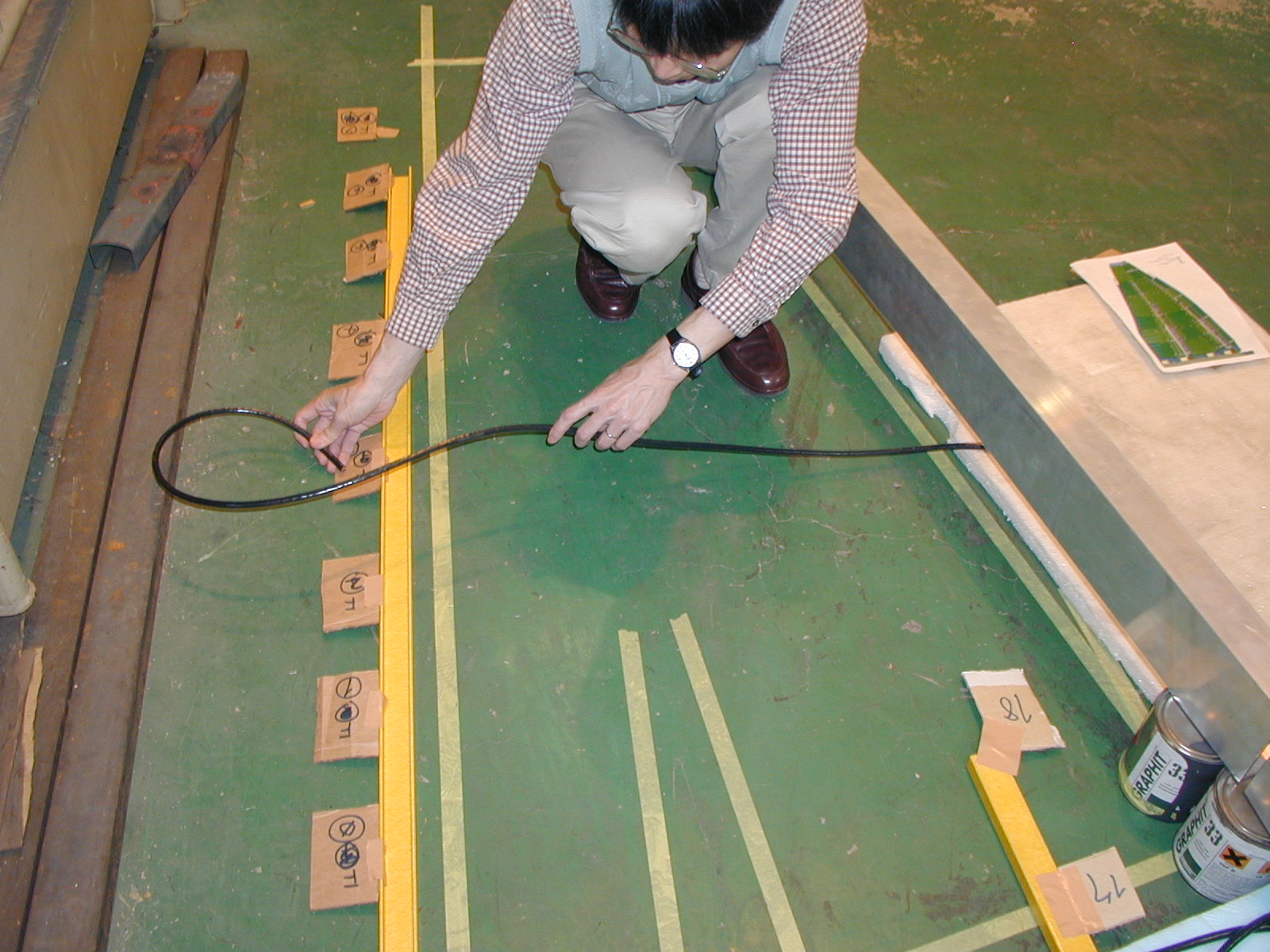
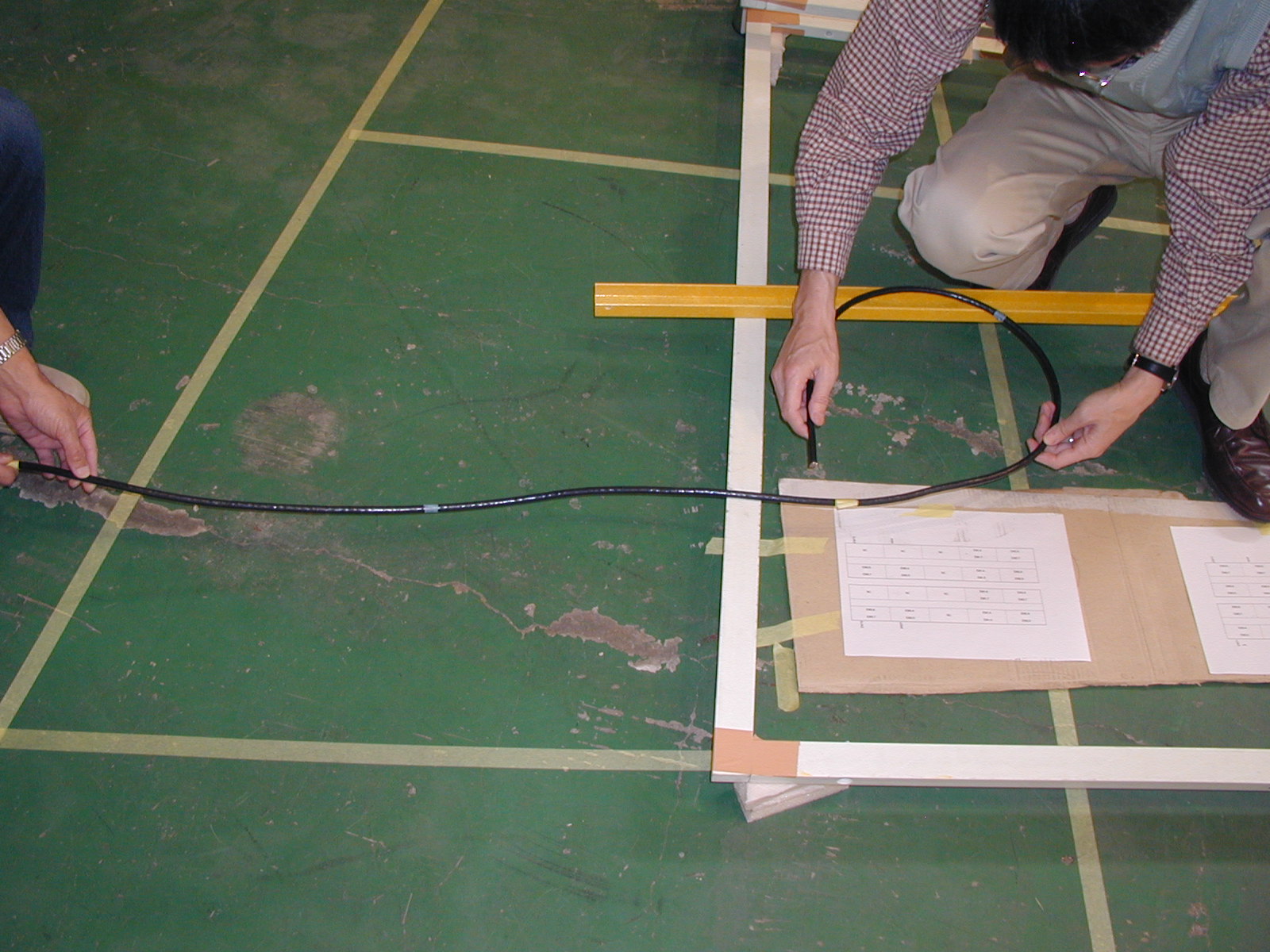
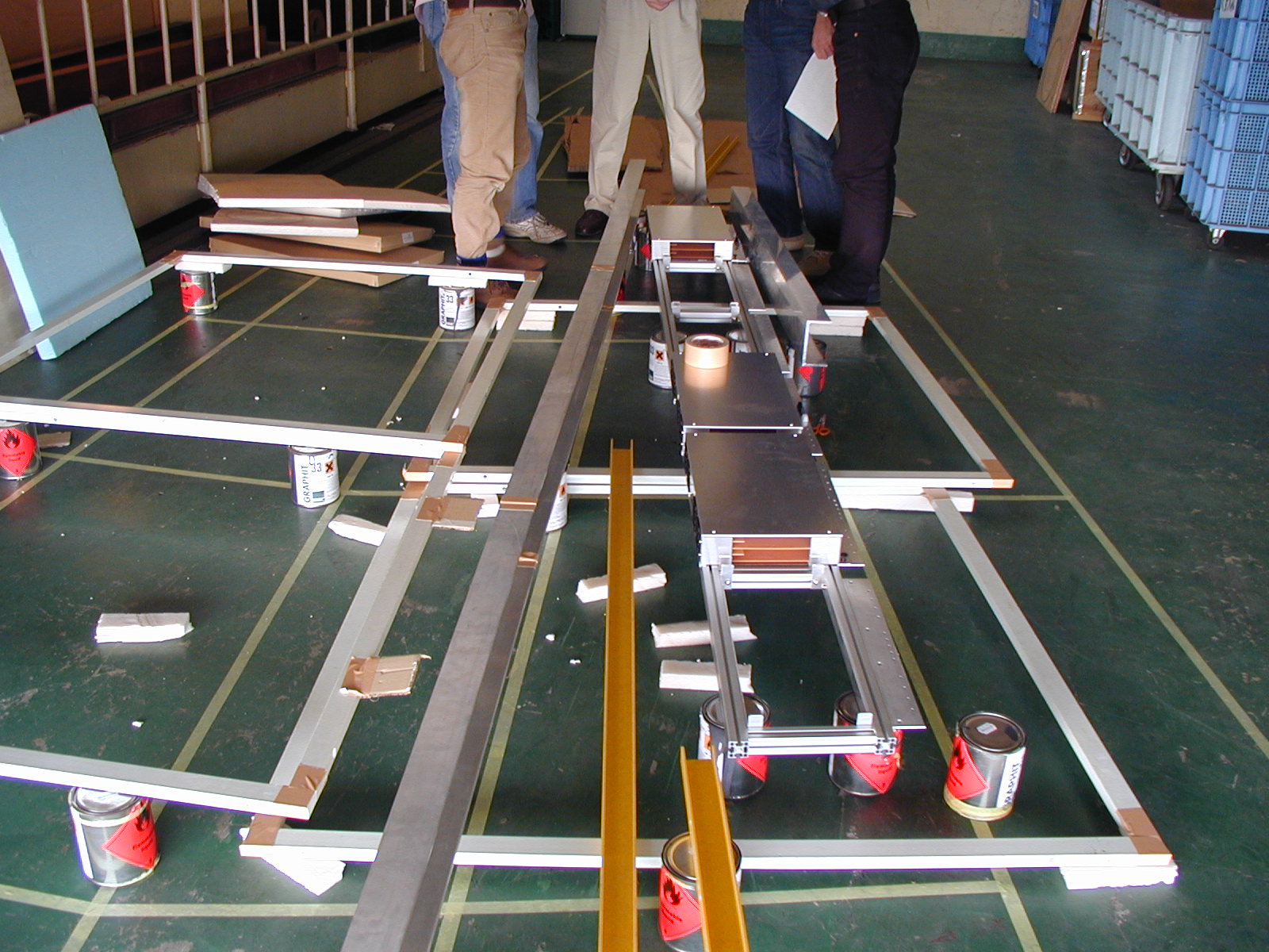
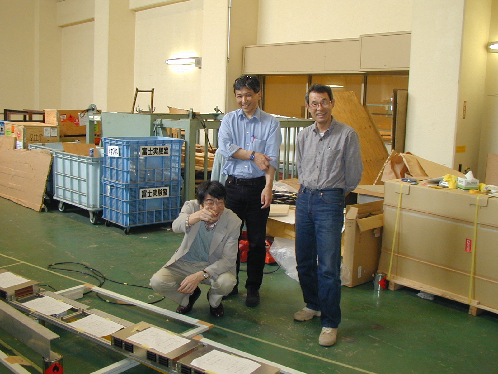
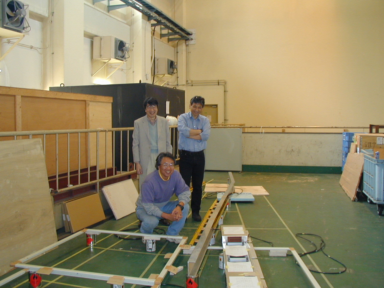
Physical cabling simulation on M3 ring has been carried out on the weekend 24 and 25/May/2003 at kek-Fuji by T.Kobayashi, T.Kawamoto, M.Nozaki and T.Takeshita with addtional contributions from H.Iwasaki, S.Tanaka and K.Ishii.
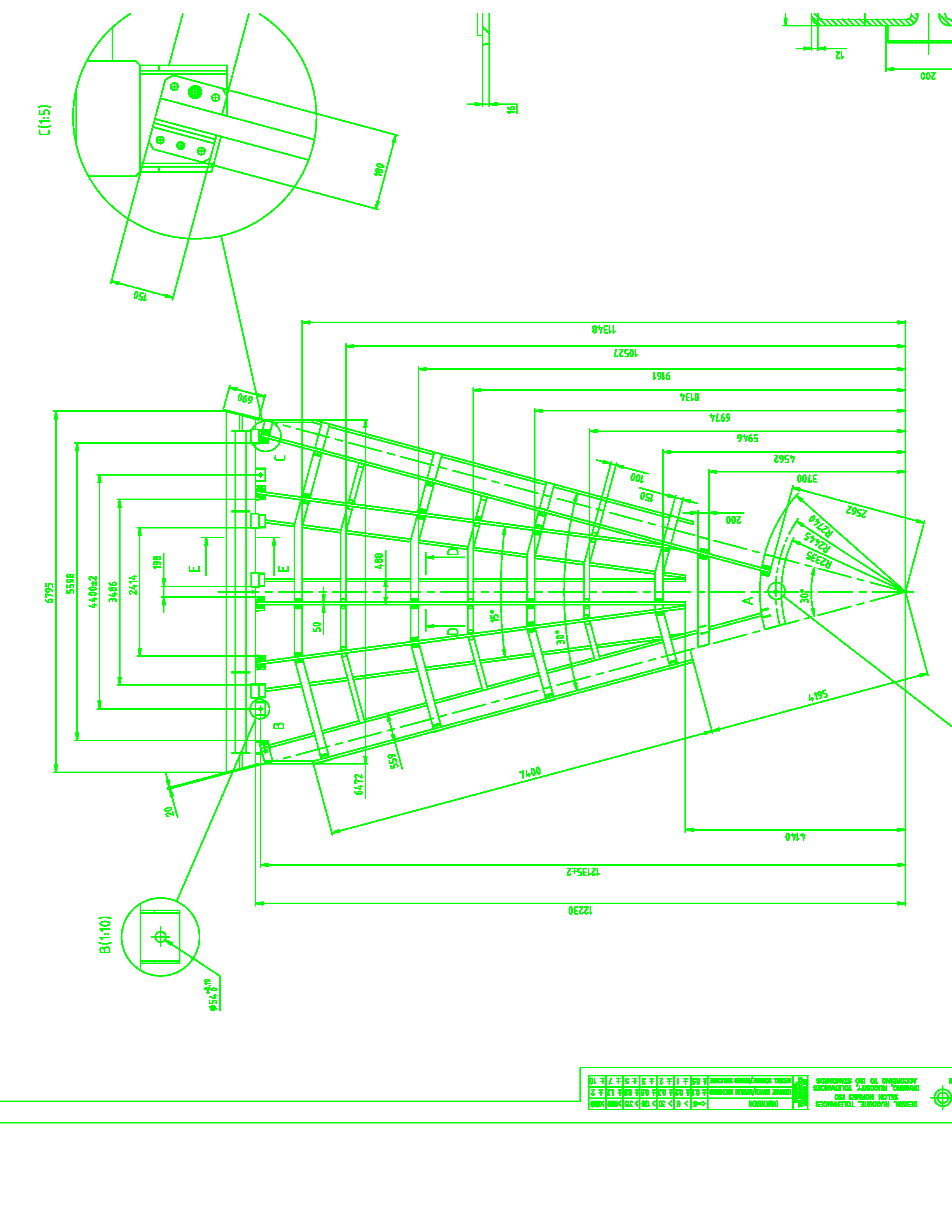
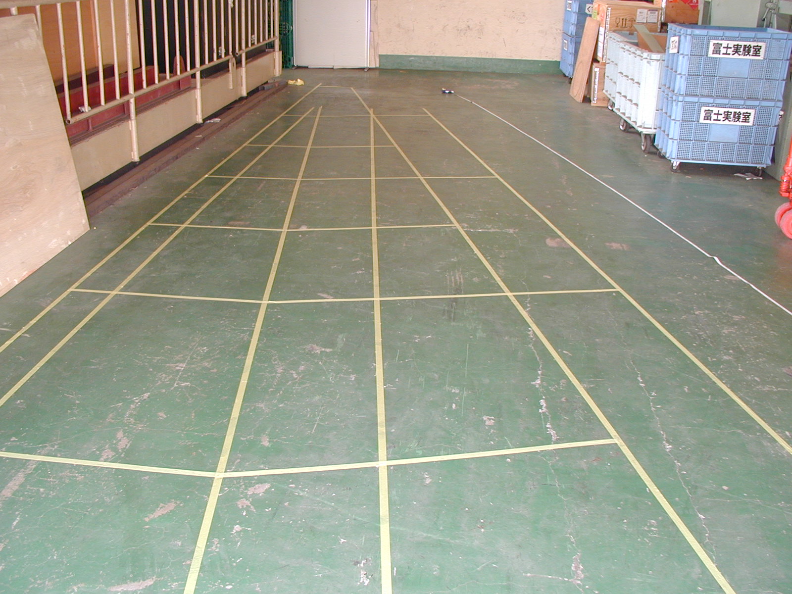
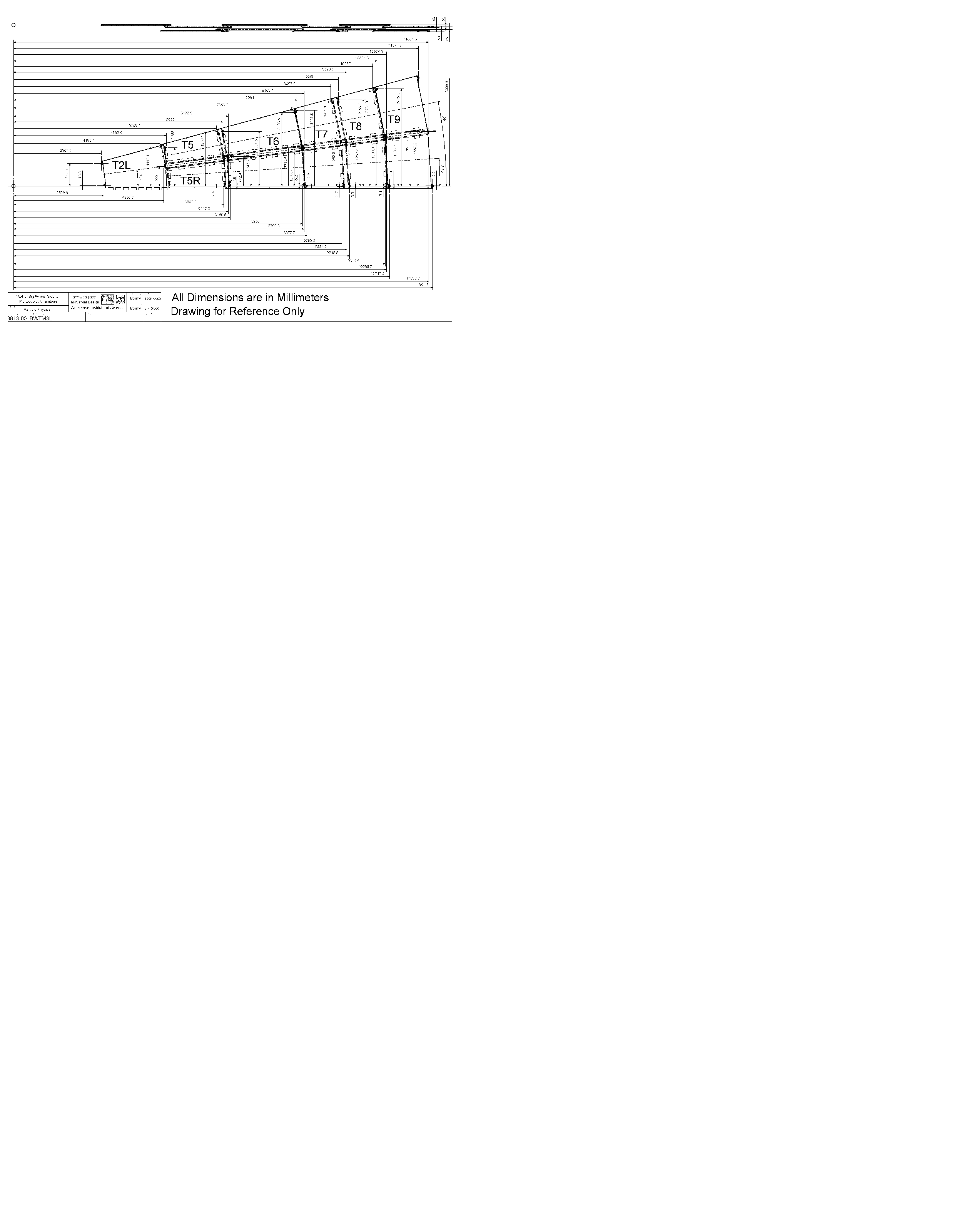
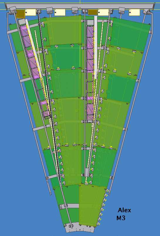
0. basic M3 structure drawing ---- picture 1 floor
3. Relative height of the Al-profile and the TGCs is set : : a view from large R and : a view from small R
4. How to install the cables : pictures !
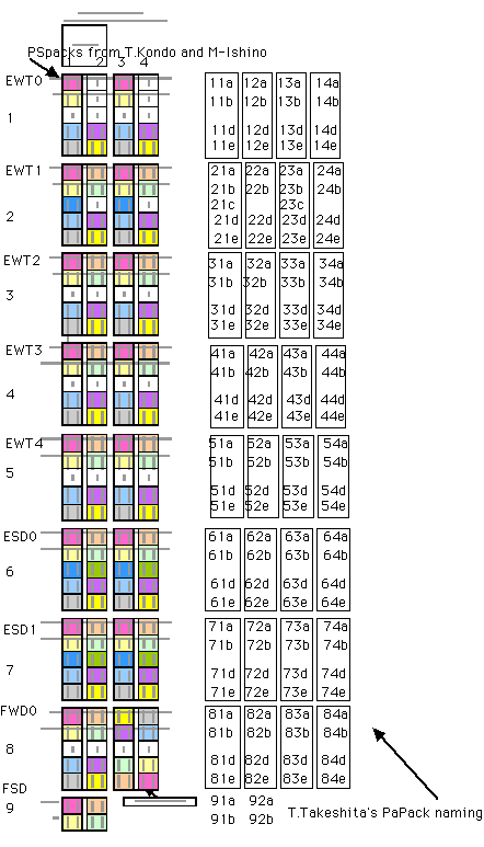
ASD = EW0 which sits farest from the beam ,
ASD = EW0 of phi 0, ASD = EW1 of phi 1 , ASD = EW1 of phi 0 , ASD = EW2 of phi 1 , ASD = EW2 of phi 0 , ASD = EW3 of phi 1 , ASD = EW3 of phi 0 , ASD = EW4 of phi 1 , ASD = EW4 of phi 0 , ASD = EW5 of phi 1 , ASD = EW7 of phi 1 , ASD = EW8 of phi 0 , ASD = EW10 of phi 0 ,
ASD = ES8 of phi 0 , ASD = ES9 of phi 1 , ASD = ES8 of phi 0 , ASD = ES7 of phi 1 , ASD = ES2 of phi 0 , ASD = ES1 of phi 0 ,
Forward Strips , Forward Wire ASD 3 , Forward Wire ASD 3 ,
from M2 patch-panel to pspack1 ,
5. results of the measured cable length a pdf or a html- tableÅ@Å@ and pspack naming in the table
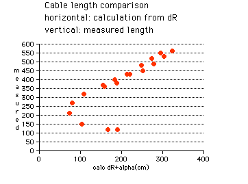
6. cable length comparison between the measured and calculated a pdf or a html- table and a plot
7. a quiz, who is who ? from the picture ?
8. cables from the Patch-Panel seem to be managed with loops in front of the PS-Pack : [1] , [2] , [3] , [4]
9. pictures of the member 1 and 2
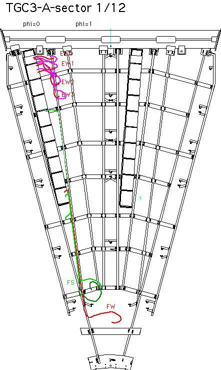
10. cable routing drawing 1
![[1]](length/cable-from-pp1.JPG)
![[2]](length/cable-from-pp2.JPG)
![[3]](length/cable-from-pp3.JPG)
![[4]](length/cable-from-pp4.JPG)